Power it from USB-C
A standard 5 V supply powers the switching circuitry directly. No battery, charging routine, firmware or host software is needed.
 ACOUSTICS
PROTOTYPE DEVELOPMENT
A compact SP4T RF switch built around the Qorvo RFSW6042. Connect a common SMA port to one of four RF paths with two simple jumpers.
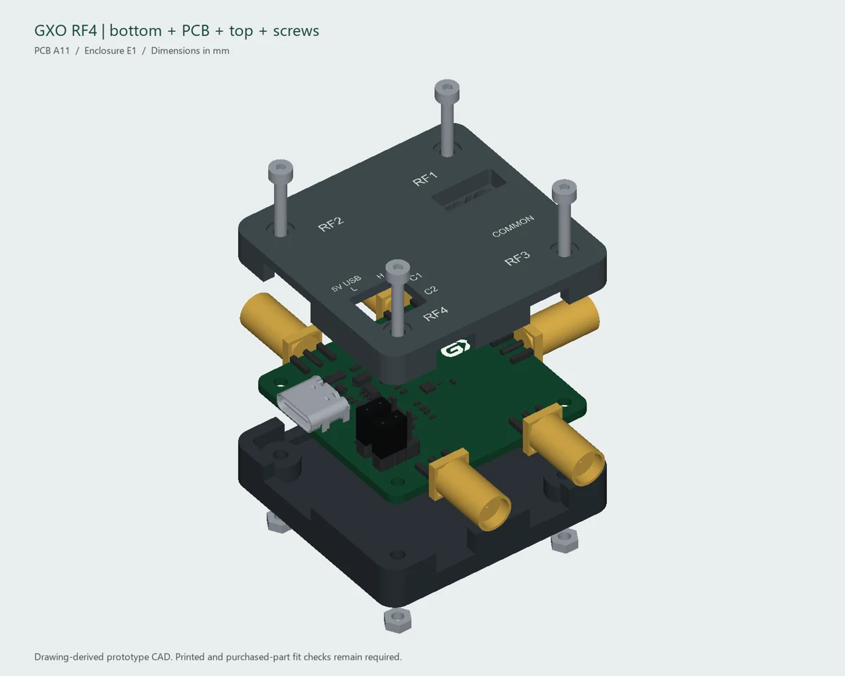
Drag to rotate · Scroll or pinch to zoom · Separate vertically to see every layer
Actual project CAD tessellation. Connector models and finishes are illustrative; physical fit awaits prototype testing.
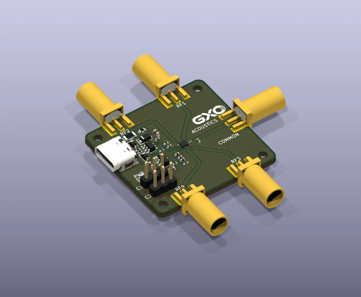
RF4 is being developed for low-power signal routing in receiver experiments and lab setups. Its selected path is bidirectional, with a 50 Ω design and five SMA interfaces.
A standard 5 V supply powers the switching circuitry directly. No battery, charging routine, firmware or host software is needed.
Choose one of four paths using C1 and C2. Clear port names and a rear selection table keep the control scheme easy to follow.
A two-layer PCB keeps fabrication cost considered. Curved traces, rounded board corners and dedicated RF return paths guide the layout.
The two-piece enclosure leaves the SMA ports and USB-C accessible. A top opening reaches both jumpers, and a GXO outline window reveals the board logo.
02 / FROM THE OUTSIDE IN
The E1 enclosure brings together a bottom shell, the RF4 PCB and a top cover, held by four M2 screws with captive nuts. The existing board mounting holes locate the assembly.
03 / DESIGN AT A GLANCE
RF4 is in prototype development. The 5 MHz–6 GHz range is a design target. Insertion loss, isolation, matching, enclosure fit and thermal behaviour still require physical verification. Commercial availability has not been announced.
04 / TWO BITS. FOUR PATHS.
Bridge LOW–BIT for L or BIT–HIGH for H on each selector. A missing shunt defaults LOW.
Mute RF before changing jumpers or power. Do not apply external DC to RF ports. Unused ports are reflective; there is no all-off state. Initial prototype testing is limited to +10 dBm CW into matched 50 Ω loads.
| C1 | C2 | Selected port |
|---|---|---|
| HIGH | LOW | RF1 |
| LOW | HIGH | RF2 |
| HIGH | HIGH | RF3 |
| LOW | LOW | RF4 Default |
FOLLOW THE DEVELOPMENT
Talk to us about your lab or receiver application.
Get in touch ↗Explore all GXO products ↗